
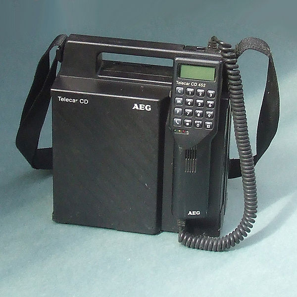
 This is what our “portable” phones looked
like! Great for staying in touch as we walked
9 miles, uphill both ways, in a snowstorm!
![]() Click any picture … (ah, you know. The cat wins the contest.)
Click any picture … (ah, you know. The cat wins the contest.)
On This Page:
“Tiny … But Fierce!“
A Non-Regulated Booster
Switch ON …
… Switch OFF
Increasing The Inductance
Duty Cycle
Continuous Conduction Mode (CCM)
Ergo Et Sum (And Didn’t Like It)
![]()
“Tiny … But Fierce!“
You’re using your new smartphone: texting, making calls and most importantly, playing games. You toss a bird into some nasty piggies — and a warning pops up:
“Your battery is low! Recharge NOW!”
This catches you by surprise, because the phone has been acting normally for hours; same brightness, same speed, same as usual.
Inside that phone, a tiny switched-mode power supply (SMPS) has been keeping the voltage(s) constant. It has dragged every ounce of available juice from that battery and has boosted it to a usable level. The battery is finally depleted, so you see that warning.
Sure, batteries have improved over the years (anyone here remember the monsters in the old cell phones)? The chips are more efficient and draw less power, too. But SMPS have improved as well.
In fact, the longer advertised “time between charge” for your new phone or tablet may be due to better, lower-power chips and a better SMPS, and not to a better battery. Read on.
 This homemade “joule thief” can keep an
LED lit for weeks on a single 1.5V AA cell.![]()
A Non-Regulated Booster
The great adventure begins. This page will have lots of graphics, because I’ll thoroughly analyze a simple boost converter. But the principles covered here will apply to everything that comes later. So … fetch a cup of coffee, wipe the flecks and specks from your display screen and let’s dig in.
Figure 2 is an LTSpice simulation that boosts a 1.5V source to 3.3V. I’ve designed for a maximum of 200mA out, with a nominal current draw of 100mA (i.e., RLoad=33 ohms*).
A few SPICE-specific notes are once again in order.
The generic passive components included with LTSpice — resistors, inductors and capacitors — are ideal, with no losses or flaws. You can right click to add things like series resistance yourself, but I haven’t bothered. The supply (V1) is also lossless (very much unlike a real-world battery).
The MOSFET (M1) and the high-speed schottky rectifier diode (D1), on the other hand, are chosen from LTSpice’s included library of actual components. These will model things like leakage and switch times.
For example: V2 drives M1 at 500KHz, and the duty cycle at the gate is 50% — 1uSec on, 1 uSec off. When the sim is run, LTSpice pulls in the model for the AO6408 MOSFET, crunches the numbers, then stretches that to about 57% “on” time at the drain.
 Fig 2: Sim schematic of a boost converter.
![]()
Now for the waveforms (figure 3), with notes added:
- The switch (M1) turns on, pulling the drain low (see the middle trace). The left side of L1 is positive. Diode D1 is reverse-biased and doesn’t conduct. C1 supplies the load with energy stored on a previous cycle.
- The inductor current ramps up, storing energy (the top trace).
- The switch turns off (middle trace); the drain goes high. Because the inductor is now dumping stored energy, the voltage polarity reverses: the right side of the coil is positive.
- The inductor current ramps down (top trace) and D1 conducts, (re)charging the filter capacitor, C1.
The bottom trace is the output voltage. At 500KHz, a relatively small capacitor does a good job of smoothing the ripple. We can use a smaller inductor, too.
 Fig 3: Waveforms from a sim run of figure 2.
![]()
Switch On …
Steady, unchanging DC in a coil won’t do anything for us (except to push the inductor closer to saturation). What counts is the change in current. In SMPS-speak, this is called the “AC ripple current.” Here’s the formula again:
A-s = V / L
… where “V” is volts, “L” is inductance in henries and “A-s” is amperes per second.
In Figure 2, we applied 1.5 volts to a 10uH inductor. Ignoring a small drop across the MOSFET, the estimated current rise should be
A-s = 1.5 / .00001 = 150,000 amps per second.
… or 150 mA per microsecond. In figure 4 (below), I’ve zoomed in. The ramp goes almost from 160 mA to 310 mA in 1 microsecond.
Remember: under ideal conditions, the rate of current rise during switch “on” is determined only by the applied voltage and the inductance.
And of course, the amount of energy added to the coil is determined by the length of the switch “on” time — the duty cycle. Remember: you can’t cheat physics. If you put energy in the coil, the same amount of energy must leave the coil eventually.
 Fig 4: 150 mA per uSec,
10 uH with 1.5 V applied.![]()
… Switch Off
That same formula applies during the “off” cycle. (Again: all we care about are changes. The AC ripple current.)
Figure 5 (below) shows that the current drops about 100mA in 500 nSec — 200,000 amperes per second. Let’s rearrange the formula to see how much voltage should appear across the coil:
V = A-s x L = 200,000 x .00001 = 2 volts.
The left side of the coil is at 1.5V; the right side is positive, so the voltages add (the coil “boosts” the input voltage; whence the name of this circuit). What is the total voltage now on the drain of M1?
source voltage + coil voltage = 1.5 + 2 = 3.5 V
The final output voltage is 3.5 V minus the diode drop. D1 is a small high-speed schottky: typically .2-.3 V. Subtract that from 3.5 to get the final output voltage (figure 3, above).

Fig 5: 200,000 amperes per second.![]()
Increasing The Inductance
If you have LTSpice, download my little test rig (figure 2, above); save it to disk, then load it into LTSpice and play with it. Right click on the values to make changes. The simulation time is set to 1mSec; you may want to increase that to give the output voltage time to settle to its final value.
Let’s compare the coil and MOSFET currents with L1=10uH, C1=10uF and L1=100uH, C1=100uF.
(I increased C1 with the larger inductance because I was getting an ugly resonance; more on that later, too.)
With a higher inductance, the peak current through M1 goes down, but the average coil current goes up. What’s interesting, though, is that the average output voltage hasn’t changed. It’s smoother with the bigger cap, but it still averages about 3.3 volts. Hmm.
 Fig 6: Increasing L1 and C1.
![]()
Duty Cycle
In a boost converter, as long as the total coil current (AC ripple + DC component) never touches zero, if we ignore other circuit losses, the output voltage is determined entirely by the duty cycle:
Vout = Vin / (1-D)
… where “D” is the “on” time (i.e., the duty cycle). For example, the actual duty cycle (on the drain of the MOSFET) in figure 3 is about 57%. So:
Vout = 1.5 / (1-.57) = 1.5 / .43 = about 3.5V.
That’s on the drain of M1; once again, you’d subtract the diode drop to get the final output voltage: about 3.3 volts.
Try this yourself in LTSpice: edit V2 so that the pulse time is 1.5uSec on, 2uSec total. That’s a “D” of 75% on the gate; when I ran the sim, M1 stretched it to about 79%. So …
Vout = 1.5 / (1-.79) = 1.5 / (.21) = about 7.14V
… very close what I saw on M1’s drain (figure 7, below).
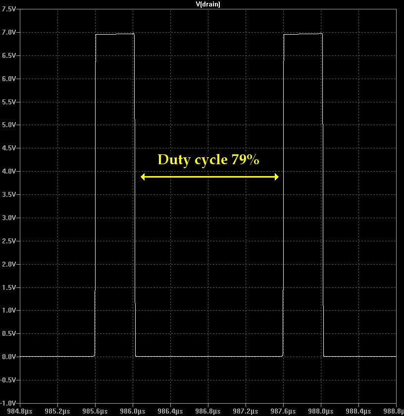 Fig 7: Increased duty cycle:
the drain voltage goes up.![]()
Continuous Conduction Mode
As long as the current in the coil never drops to zero, you’re in what the SMPS-geeks call “Continuous Conduction Mode,” or CCM. The formula I just showed you, Vout = Vin / (1-D), is only valid in CCM.
If the coil current does drop to zero, that’s called “Discontinuous Mode” (DCM), and it requires more complicated math. DCM is fine for ultra-small regulators (such as those in smartphones), but for our experiments, we can stay (or at least start) with CCM.
Here comes a convoluted example, but if you stick with it, you’ll win one (1) splendid set of waveforms that you can print and frame for display. (Amaze your friends and loved ones.)
In figure 8, L1 is back to 10uH. I’ve lengthened the simulation time and I’ve replaced that fixed resistive load with an active one (ILoad, to the right). The load starts by drawing 200mA, or design maximum. It then smoothly decreases to 2mA by the end of the sim run.
(I also left in the 100uF cap because I liked it, so there. Here’s the sim schematic if you want to play with it.)
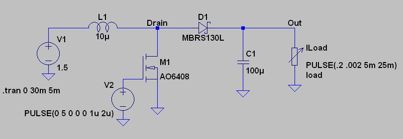 Fig 8: Using an active, variable load.
![]()
The waveforms are shown next (figure 9, below). Remember that we start at full load (200mA) and lighten the load as you move from left to right. The load current is shown in the third trace (“ILoad”) for reference.
The top trace, I(V1), is the source current from our 1.5V “battery.” Not surprisingly, it decreases as we lighten the load. The input power must at least equal the output power (and in real life, of course, the input will be somewhat higher because of less than 100% efficiency).
I(L1), the coil current and V(out), the output voltage, are more interesting. Sure enough, the output voltage stays close to 3.3V until the bottom of the coil current waveform starts touching zero. Then it takes off, headed up.
Note that the width of the red AC ripple trace doesn’t change. Again: the “rise” (i.e., “on”) slope is determined entirely by the applied voltage and inductance.
The “fall” or switch “off” slope, on the other hand, can get complicated, especially if you’re not in continuous conduction — i.e., you’re using a very light load for the inductor size. The value of C1 isn’t critical, but you do want a time constant that’s many times longer than the pulse width.
(Try the sim with a 100K load and no filter cap — i.e., delete C1 entirely. The peak voltage on the drain of M1 will be very much higher.)
 Fig 9: The waveforms from a sim run of figure 8.
![]()
Ergo Et Sum (And Didn’t Like It)
It’s time for a break to briefly summarize what I’ve shown you here.
I didn’t specifically say this above, but the boost converter can only make an output voltage that’s higher than the input. Also, it can be made very efficient, but there is one glaring drawback: there’s no short-circuit protection (because the input voltage can always find a path through the inductor). You’ll need to protect your circuit some other way.
The input power will also be equal to the output power plus the losses in the switching circuit. The difference between the two, of course, is the efficiency.
The current rise and fall (the change) in the coil, vs. the voltage across the coil obeys this formula:
A-s = V / L.
As long as the current in the coil remains above** zero, the output is essentially determined by the duty cycle:
Vout = Vin / (1-D)
Click here for the next page, where we’ll look at a real-life boost supply using one of Linear Technology’s chips. (The fact that the actual circuit would fit on a dime — see below — is just a bonus.)

Red is the inductor, blue is the
capacitor and resistors are green.
The black chip is the regulator. It
all fits neatly on a single US dime.![]()
*For the curious: if you’re setting up your own simulation, simply choose an inductor that has a reactance equal to the nominal output impedance — 33 ohms in this case. That’s a good start. Play with your sim and adjust as needed.
**If I’m going to be strictly accurate, I should say, “as long as the absolute value of the coil current stays above (or away from) zero.” But you’re smart enough to realize that.